I use MSP430F5529 to control ADS1292R, it converted data in continuous mode,
But the timing seems to have a problem.
Below is a screenshot of the oscilloscope, the first (red line) is the DRDY signal, the third (green) is the SCLK signal.
Image may be NSFW.
Clik here to view.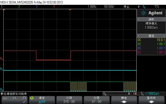
Image may be NSFW.
Clik here to view.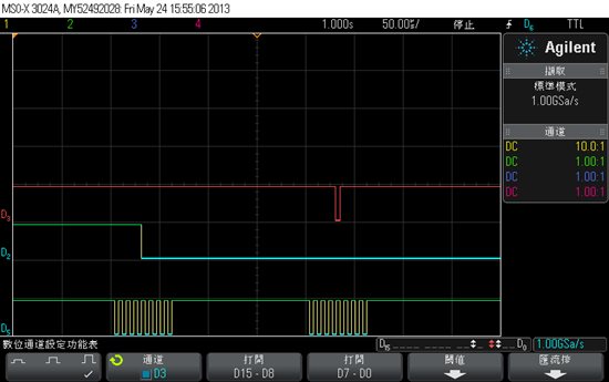
Image may be NSFW.
Clik here to view.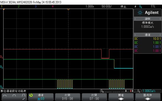
the command read back currently is right, which means that the command has write into it.
But my DRDY is still not periodic square wave, and the position of the falling edge is not correct.
My program is according to datasheet p.63 written, I do not know what went wrong. I would like to ask what the problem,
thanks!
int main(void) {
WDTCTL = WDTPW | WDTHOLD; // Stop watchdog timer
unsigned char dat[3];
// CLK setting
UCSCTL3 |= SELREF_2; // Set DCO FLL Reference = REFO
UCSCTL4 |= SELA_2; // Set ACLK = REFO
__bis_SR_register(SCG0); // Disable the FLL Control Loop
UCSCTL0 = 0x0000; // Will be Set Automatically by FLL
UCSCTL1 = DCORSEL_2; // 1 MHz range
UCSCTL2 = FLLD_1 + 32; // Set FLL to approximately 1 MHz:
// FLL divider result = 32768
// 64 * 32768 = "2 MHz"
// set related pins with ADS1292R
P2DIR |= BIT3; // P2.3 -> CLK_SEL
P8DIR |= BIT0 + BIT1 + BIT2; // P8.0 -> RESET, P8.1 -> START, P8.2 -> CS'
// SPI initialization
P3SEL = BIT0|BIT1|BIT2; // Set Pin Function for SPI Mode
UCB0CTL1 |= UCSWRST; // **Put state machine in reset**
UCB0CTL0 |= UCMST+UCSYNC+UCCKPL+UCCKPH+UCMSB; // 3-pin, 8-bit SPI master
// Clock polarity high, MSB
UCB0CTL1 |= UCSSEL_2; // SMCLK
UCB0BR0 = 0x02; // /2
UCB0BR1 = 0; //
UCB0MCTL = 0; // No modulation
UCB0CTL1 &= ~UCSWRST; // **Initialize USCI state machine**
// indicate ADS1292R use internal clock
P2OUT = BIT3; // indicate ADS1292R use internal clock
__delay_cycles(100); // wait for oscillator to wake up
// wait for 1s for ADS1292R's power-on reset
P8OUT |= BIT0; // set RESET'=1
delay_ms(1000); // wait for 1s for power-on reset
// reset ADS1292R & CS' pin tied low
P8OUT &= ~BIT0; // issue reset pulse
delay_ms(100); // wait 0.1s
P8OUT |= BIT0; // clear reset
P8OUT &= ~BIT2; // CS' tied permanently low
// send command
Send_CMD(0x11); // sent SDATAC command
dat[0]=0xA0; // CONFIG2 = A0;
Send_CMD_Multi(0x40+0x02, 1, dat); // Config. CONFIG2 = 0xA0 to use internal reference
dat[0]=0x2C; // RLDSENS = 2C;
Send_CMD_Multi(0x40+0x06, 1, dat); // right leg drive
dat[0]=0xC2; // RESP1 = C2;
Send_CMD_Multi(0x40+0x09, 1, dat); // turn on RESP demodulation&modulation
// DRDY' interrupt
P1IE |= BIT0; // P1.0 interrupt enabled
P1IES |= BIT0; // P1.0 Hi/lo edge
P1IFG &= ~BIT0; // P1.0 IFG cleared
// START = 1
P8OUT |= BIT1; // START = 1
// send continue mode command
Send_CMD(0x10); // enter the continue mode
__bis_SR_register(LPM0_bits + GIE); // CPU off, enable interrupts
return 0;
}