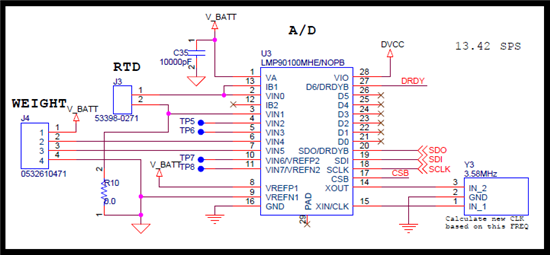
Hi, I'm working with the LMP90100 and am running into a problem I was hoping to get some help with. The IC works beautifully on channel 0 (an RTD connected channel) but when I take data from Channel 1, currently the only other channel in use, I get a value that is consistent withing the board, and does not change with an input. The value that the LMP90100 is "stuck" on varies between boards. SPI communications work, I have written and verified registers, and as I said before another channel is behaving correctly. My connections are below:
My register settings look like this:
0xC3, //RESETCN: Set to reset on startup to clear old data
0x00, //SPI_RESET: SPI reset (not RESETCN) is disabled
0x00, //start in active mode //0x01, //PWRCN: Start in power down mode. Woken when needed
0x00, //ADC_RESTART: Nothing to restart on start-up, cleared for initialize
0x10, //ADC_AUXCN: Calibration registers not cleared on reset, external clock enabled, RTD Current initialize to 0 uA, will be turned on for reading only
0xFF, //ADC_DONE-no data available at start
0x00, //CH_SCAN: Continuous scan, single channel. LAST_CH = 0, FIRST_CH = 0
0x01, //CH0_INPUTCN: No Burnout Current (diagnostics disabled because of the error it would
//introduce. If necessary, error potentially solved by putting in continuous
//and shutting off after one cycle) VREFP/N 1 selected VINP = VIN0, VINN = VIN1
0x46, //CH0_CONFIG, ODR min for data reliability to reduce on-time for current source, gain = 8,
//buffer enabled automatically, can be disabled to save power at cost of precision
0x25, //CH1_INPUTCN: VINP = 4, VINN = 5, rest same as CH0
0x4F, //CH1_CONFIG: ODR Max, Gain = 128, variation of strain gauge = 7.2mV variation from 0 to max.
//buffer off
0x00, //CH2_INPUTCN: Don't Cares
0x70, //CH2_CONFIG: Don't Cares
0x00, //CH3_INPUTCN: Don't Cares
0x70, //CH3_CONFIG: Don't Cares
0x00, //CH4_INPUTCN: Don't Cares
0x70, //CH4_CONFIG: Don't Cares
0x00, //CH5_INPUTCN: Don't Cares
0x70, //CH5_CONFIG: Don't Cares
0x00, //CH6_INPUTCN: Don't Cares
0x70, //CH6_CONFIG: Don't Cares
0x00, //BGCALCN: off, Gain and Offset Correction will likely be used in a manual calibration for upkeep to be implemented at a later stage
0x00, //CH0_SCAL_OFFSETH-restore to default
0x00, //CH0_SCAL_OFFSETM-restore to default
0x00, //CH0_SCAL_OFFSETL-restore to default
0x80, //CH0_SCAL_GAINH-restore to default
0x00, //CH0_SCAL_GAINM-restore to default
0x00, //CH0_SCAL_GAINL-restore to default
0x01, //CH0_SCAL_SCALING-restore to default
0x00, //CH0_SCAL_BITS_SELECTOR-restore to default
0x00, //CH1_SCAL_OFFSETH-restore to default
0x00, //CH1_SCAL_OFFSETM-restore to default
0x00, //CH1_SCAL_OFFSETL-restore to default
0x80, //CH1_SCAL_GAINH-restore to default
0x00, //CH1_SCAL_GAINM-restore to default
0x00, //CH1_SCAL_GAINL-restore to default
0x01, //CH1_SCAL_SCALING-restore to default
0x00, //CH1_SCAL_BITS_SELECTOR-restore to default
//0x00, //SCALCN-default normal mode
// offset and gain registers are here in the datasheet. Not written because it will likely be needed
//later for a manual calibration
0x00, //SENDIAG_THLD: Set to 0 because the weight sensor may be quite close in value (near 0 difference)
//when no weight, this is not a short, can be revisited to look at RTD
0x00,
0x07,//SPI_HANDSHAKECN: DRDYB is driven by the slave, this will allow the mcu to enter low power mode while waiting for
//the conversion. DRDYB is connected to an external interrupt.
0x00, //SPI_STREAMCN: used in streaming mode- controlled streaming, range 2
0x1A, //DATA_ONLY_1: Data only transaction start address is 0x1A (default value)
0x02, //DATA_ONLY_2: Data only transaction reads out 3 bytes
0x83,//disable fga correction //0x8B, //SPI_DRDYBCN: DRDYB enabled on D6, FGA gain error is used with the last known coefficients (background cal is no
//good in single scan mode)
0x00, //SPI_CRC_CN: CRC disabled, A/D operates without it
0x40,//D6 out, rest in//0x7F, //GPIO_DIRCN: all configured as outputs, D6 is DRDYB already, rest will be set low to conserve power
0x40//set D6 high, ignore others //0x00 //GPIO_DAT: all GPIO cleared to save power
I've set the data output rate pretty low temporarily to be sure the mcu can keep up with the A/D while I'm dealing with this. I'm hoping for some help because I'm pretty stumped and would like to move on to the next stage of development asap.